
YMX filters started to make the photo etching filter screen since 2004. The reason we started this new screen is we find more and more customers are requiring a thinner plate screen and smaller holes on the sheets as a filter materials. The photo etching process could make a filter product that a woven mesh of perforated metal are not suitable.
What is photo etching?
Photo etching, also known as chemical etching or metal etching, is a highly precise, tightly controlled corrosion process used to produce complex metal components with very fine detail.
Why use photo etching?
The photo etching process offers a cost-effective alternative to stamping, punching, laser and waterjet cutting when machining precision components from thin gauge metals – up to 1.5mm thick – including stainless steel, nickel and nickel alloys, aluminium, copper and copper alloys and hard-to-machine metals such as titanium.
When component integrity is critical, photo etching is often the only suitable metal machining technology as metal temper and magnetic properties are unaffected.
 The photochemical etching Process
The photochemical etching process consists of several steps. Each step is a critical prerequisite to the next. Although companies that produce parts using the PCM process have unique and sometimes proprietary methods to achieve the final goal, the basic operations are similar.
Photo-tool Design
The first step is to make a working tool by a film, as opposed to the “hard” tools used in metal stamping. When a new part is ordered, a photo tool must be created to profile the part. YMX Filters can create a photo tool either from a dimension drawing supplied by the customer, or by working with a customer-supplied CAD file with detailed dimensions. Once the CAD file has been received, Our tooling engineers will redraw the part entirety, modifying the dimensions to compensate for the unique characteristics of the etching process. (All features must be compensated for surface and lateral etching, which happen simultaneously during the etching process.)
Once the image is completed, it is arrayed over an area specified by the tooling engineer to maximize the number of units per sheet of metal. After that, the image is sent to a laser photo-plotter and is created on a piece of Mylar film, which is then developed. If all features on both sides of the part are identical, a duplicate film is created; if not, a second piece of film is developed and aligned with the first. Holes are punched in the two pieces of film and they are aligned top to bottom. Registration holes are punched in both pieces of film. This is critical to prevent misalignment of the film during subsequent processing.
Material Preparation
Once the material has been cut to the specified sheet sizes, it’s chemically cleaned to remove all foreign debris, dusts, grease, oil and other contaminants from the surface so that the photo resist can adhere to the metal.
Coating
The next step in the process is the application of photo resist. We call it as “the coating operation.” The coating operation is exactly what it sounds like – film photo resist is rolled onto the cleaned metal sheets using a hot-roll lamination system. At this point in the process, the sheets of metal are processed in a yellow safe-light environment.
While we typically coats both sides of a metal sheet previously cut to size, in some cases, metals in thinner gauges can bypass the prep process and the resist can be applied to the entire coil. This is because thinner gauge material is generally clean of contamination, and will not be exposed to the harsh chemistry long enough for the photo resist to fail. Once the sheet or coil is coated with photo resist all edges are trimmed of the excess. At this point the material is ready for exposure.
Printing/Imaging
In this area, the photo tool image is transferred to the metal sheet by activating the polymer within the photo resist. The metal sheet is sandwiched between two pieces of film (the photo tool), the operator creates a vacuum to prevent air bubbles and ensure that there are no gaps between the photo tool and the metal. The panel is then exposed to UV light.
The areas on the photo tool that prevented the UV light from seeing the photo resist will not harden or cure, so an image is formed in the photo resist. Once the photo tool has been printed onto the metal sheet, it is ready to move into the wet process area for developing.
Developing
All sheets that have been coated and exposed must go through a conveyorized developing system. The unexposed areas of the photo resist are rinsed off in a high-pressure alkaline solution, exposing the bare metal and leaving resist on those areas that have to be protected from the etchant. The developing process forms an adherent, durable image on both sides of the metal, which is now ready for the etching process.
Etching
The metal sheets are placed in a large conveyorized spray system that sprays them from both sides with the appropriate etch chemistry, dissolving the bare metal. The speed of the conveyor is carefully calibrated so when the sheets approach the final rinse chamber, they are completely etched through and all dimensions are held within specified tolerances.
After etching and rinsing, the sheets are ready to have the photo resist stripped off.
| Base Material | Etchant |
| Ferrous alloys (stainless steel, kovar, etc.) | Ferric Chloride |
| Non-ferrous alloys (brass, nickel-silver, beryllium copper, etc.) | Cupric Chloride |
| Titanium and zinc and their alloys | Copper Based Proprietary Etchant |
| Molybdenum and silver | Ferric Nitrate |
| Gold and gold alloys | Iodine-Based Etchant |
Stripping
The etched metal sheets still have the photo resist remaining on the un-etched portions. They are either tank-stripped, or stripped on a 30-foot conveyorized spray stripper. The resist is removed using a sodium hydroxide-based solution, and once stripped, the sheets are cleaned in water, then rinsed in water and dried.After the photo resist has been removed, the parts or sheets go on to be inspected and packed for shipment to the customer or prepared for secondary operations such as plating, forming, lapping, welding, soldering, etc.
YMX FILTER MANUFACTURING CO., LTD
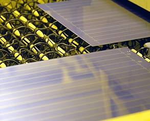 Etching Process
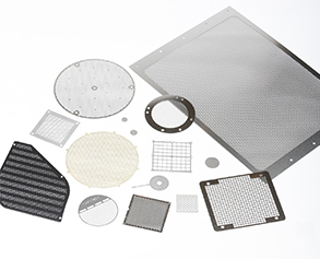 Fotofab
 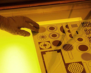 Photo Chemical Etching Process
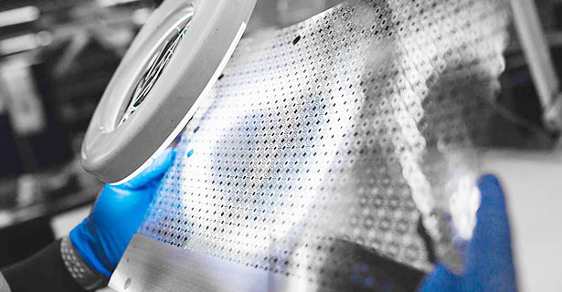
 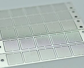 Photo Etching Screen
Inspection, Packaging & Shipping:
PEI prides itself on providing the highest level of Quality for all products we produce. Every new part that is etched requires a very careful inspection before production is released. We inspect to industry standards (Military/Aero, Medical or other) but will gladly establish a custom inspection plan designed specifically to satisfy all our customer expectations.
